FPGA falsh相关知识总结
1.存储容量是128M/8 Mb=16MB
2.有256个sector扇区*每个扇区64KB=16MB
3.一页=256Byte
4.页编程地址=0+256
5:在调试SPI时序的时候一定注意,miso和mosi两个管脚只要没发送数据就一定要悬空(处于高组态),不然指令会通过两个管脚进入主从机里面。
6.如果通过串口实现远程升级,都是按照页编程(256B),如果遇到256的非整数倍后面直接用FF代替(可行),用0代替(有待验证)。
7.flash的读指令必须要能正确读出数据,必须要首先在前几个状态机给出擦除操作。
8.编程底层flash驱动需要用到
STARTUPE2 原语
STARTUPE2  #(
    .PROG_USR("FALSE"), // Activate program event security feature. Requires encrypted bitstreams.
    .SIM_CCLK_FREQ(0.0) // Set the Configuration Clock Frequency(ns) for simulation
)
STARTUPE2_inst
(
    .CFGCLK(), // 1-bit output: Configuration main clock output
    .CFGMCLK(), // 1-bit output: Configuration internal oscillator clock output
    .EOS(), // 1-bit output: Active high output signal indicating the End Of Startup.
    .PREQ(), // 1-bit output: PROGRAM request to fabric output
    .CLK(0), // 1-bit input: User start-up clock input
    .GSR(0), // 1-bit input: Global Set/Reset input (GSR cannot be used for the port name)
    .GTS(0), // 1-bit input: Global 3-state input (GTS cannot be used for the port name)
    .KEYCLEARB(1), // 1-bit input: Clear AES Decrypter Key input from Battery-Backed RAM (BBRAM)
    .PACK(1), // 1-bit input: PROGRAM acknowledge input
    .USRCCLKO(flash_clk), // 1-bit input: User CCLK input
    .USRCCLKTS(0), // 1-bit input: User CCLK 3-state enable input
    .USRDONEO(1), // 1-bit input: User DONE pin output control
    .USRDONETS(1) // 1-bit input: User DONE 3-state enable outpu
);
九:VIVADO 擦除flash 流程
1.MCS和PRM文件(如program就只需MCS即可)
2.完整的配置存储器设备
3.只选erase
4.其他默认不勾选
十:FPGA程序执行相关知识点
1.目前,大多数FPGA芯片是基于 SRAM 的结构的, 而 SRAM 单元中的数据掉电就会丢失,因此系统上电后,必须要由配置电路将正确的配置数据加载到 SRAM 中,此后 FPGA 才能够正常的运行。
常见的配置芯片有EPCS 芯片 (EPCS4、EPCS8、EPCS16、EPCS64、EPCS128),还有通用的串行 SPI FLASH 芯片如 M25P40、 M25P16、 W25Q16 等。
配置(configuration)是对FPGA的内容进行编程的过程。每次上电后都需要进行配置是基于SRAM工艺FPGA的一个特点,也可以说是一个缺点。FPGA配置过程如下:
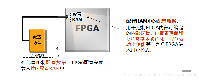
2.在线烧录程序文件(bit/elf)——相当于把程序放在SRAM去执行,掉电程序无。
3.固化——相当于把程序放在flash去,上电FPGA会自动去flash里面拿固化的程序(配置芯片),掉电程序依然有。
十一:远程升级,从gloden区跳转到updata区
1.远程升级的思路(实验成功):
在flash的0地址固化带有接收远程升级程序(如串口接收功能)/和往flash里面写数据功能且能引导到flash的固定地址的程序(如QSPI)/和接收跳转到flash的固定地址启动(利用原语)指令。
2:流程
设备上电——FPGA自动从flash的基地址拿先前固化好的程序——通过串口往falsh里面写升级程序,并且修改跳转flash地址(最新升级的新程序)的指令。
设备断电——在启动上电——FPGA自动去之前设定好的flah跳转地址拿最新的升级程序——如果拿取失败就会自动加载旧版固化在flash的程序。
3:工具
1.所需ip核:QSPI+UART+ARM架构cpu
2.首先往flah里面固化bit+elf(bootloader),可以从flash的地址0开始固化(mcs文件生成处可以选择)。
3.上电从flash拿合并程序,并运行bit+elf(bootloader)
4.在bootloader程序里的设置写flash的地址:就是意味着往flash的哪个地址去写并引导app程序的启动。
五.需要用到的原语(从golden区跳转到update区)
1.主要就是对原语的几个信号进行操作
//   ICAPE2    : In order to incorporate this function into the design,
//   Verilog   : the following instance declaration needs to be placed
//  instance   : in the body of the design code.  The instance name
// declaration : (ICAPE2_inst) and/or the port declarations within the
//    code     : parenthesis may be changed to properly reference and
//             : connect this function to the design.  All inputs
//             : and outputs must be connected.

//  <-----Cut code below this line---->

   // ICAPE2: Internal Configuration Access Port
   //         Artix-7
   // Xilinx HDL Language Template, version 2019.1

   ICAPE2 #(
      .DEVICE_ID(0'h3651093),     // Specifies the pre-programmed Device ID value to be used for simulation
                                  // purposes.
      .ICAP_WIDTH("X32"),         // Specifies the input and output data width.
      .SIM_CFG_FILE_NAME("NONE")  // Specifies the Raw Bitstream (RBT) file to be parsed by the simulation
                                  // model.
   )
   ICAPE2_inst (
      .O(O),         // 32-bit output: Configuration data output bus
      .CLK(CLK),     // 1-bit input: Clock Input
      .CSIB(CSIB),   // 1-bit input: Active-Low ICAP Enable
      .I(I),         // 32-bit input: Configuration data input bus
      .RDWRB(RDWRB)  // 1-bit input: Read/Write Select input
   );

   // End of ICAPE2_inst instantiation
2.一定注意(如下图第四点是固化到falsh的update区的首地址(即是更新程序的mcs文件的首地址))——实测不需要在XDC里面约束这个地址
设定值的时候一定要是整数(如A00000=10MB)不然没法跳转到最新程序如(160160=1.37M)
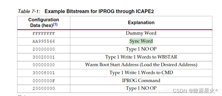
3.还需主要 key信号:代表跳转命令需要电平1——0——1(按键)
4.还需主要:csib信号和rdwrb同时拉低。