【Altera】Cyclone10 FPGA DDR3使用
目录
开发板
硬件
框图
原理图
测试工具
DDR IP核配置
调试及遇到的问题
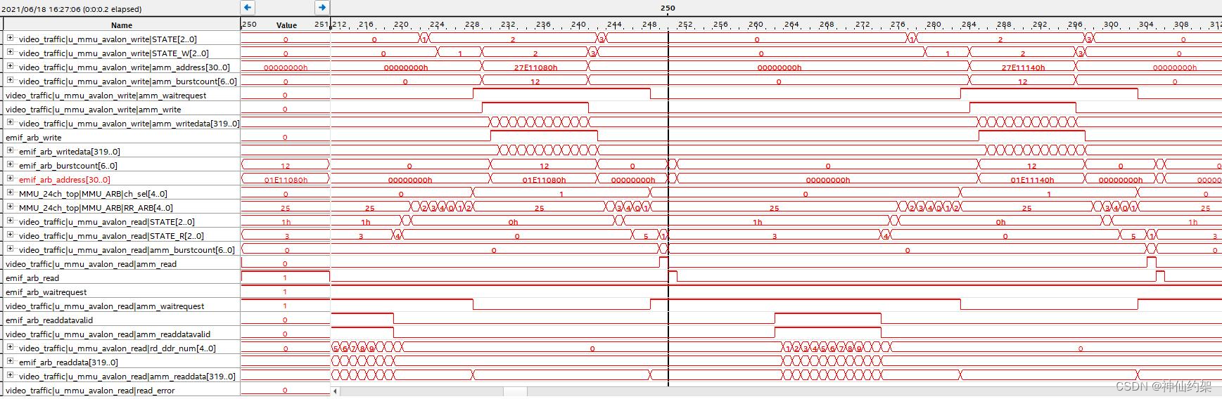
读写仲裁时序
问题1.拉高read后,wait一直没反应
问题2.DDR校正不过的一个可能性
延伸学习
开发板
Intel官方提供c10的开发套件:Intel® Cyclone® 10 GX FPGA Development Kit,很有参考价值。
官方手册
《Intel® Cyclone® 10 GX FPGA Development Kit User Guide》
《c10gx-dev-SDI-SCH》
硬件
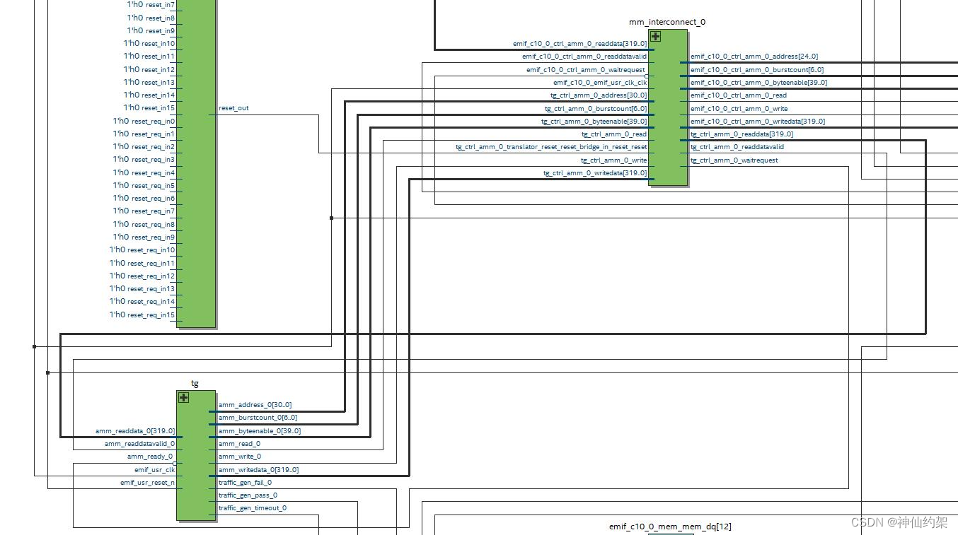
框图
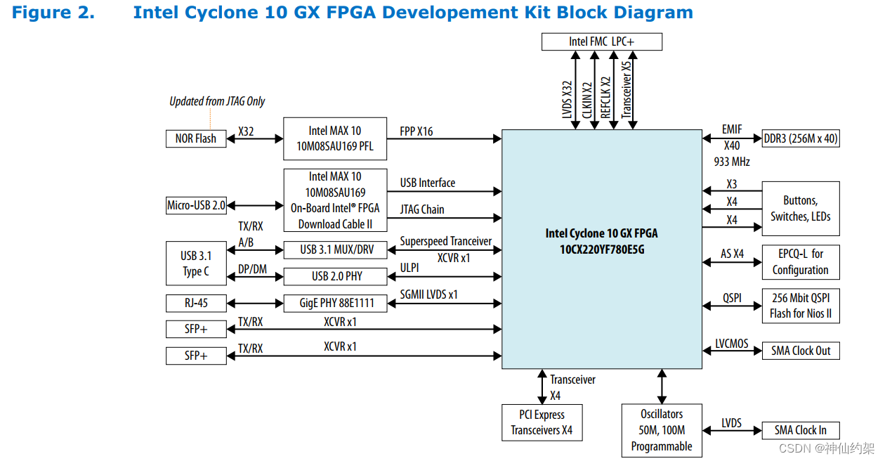
图中可见EMIF接口位宽40bit,933MHz。
英特尔Cyclone 10 GX FPGA器件支持高达933 MHz的DDR3内存。在此开发套件中,使用DDR3器件实现了933 MHz的DDR3 x40。EMIF在同一列中使用连续的bank。为了达到933 MHz的速度,EMIF使用bank 2J和2K来支持933 MHz的40位宽度。信号定义符合EMIF约束。
原理图
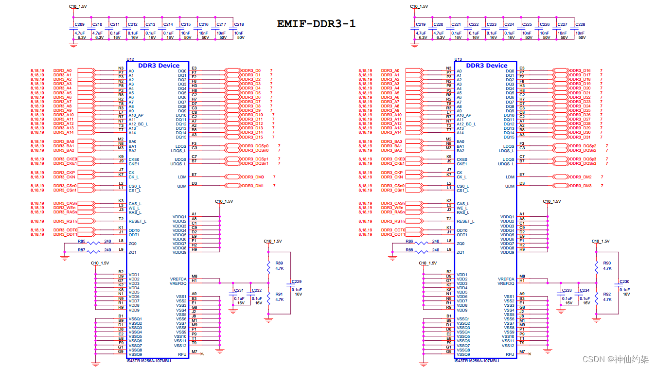
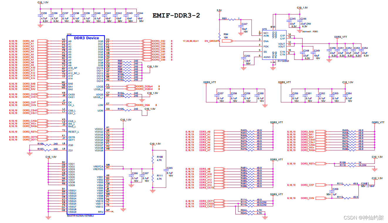
由图可见共使用了3片IS43TR16256A-107MBLI,有一片只使用了8bit,所以共16+16+8=40bit。
测试工具
官方提供测试程序Board test system,可测试ddr
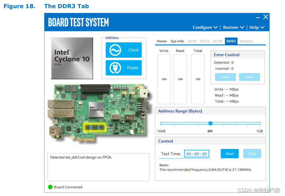
The following sections describe the controls on the DDR3 tab.
Start
Initiates DDR3 memory transaction performance analysis.
Stop
Terminates transaction performance analysis.
Performance Indicators
These controls display current transaction performance analysis information collected
since you last clicked Start:
• Write, Read and Total performance bars: Shows the percentage of maximum
theoretical data rate that the requested transactions are able to achieve.
• Write (MBps), Read(MBps) and Total(MBps): Show the number of bytes of
data analayzed per second.
Error
ControlThis control displays data errors detected during analysis and allows you to inserterrors:
• Detected: Displays the number of data errors detected in the hardware.
• Inserted: Displays the number of errors inserted into the transaction stream.
• Insert: Inserts a one-word error into the transaction stream each time you click
the button. Insert Error is only enabled during transaction performance analysis.
• Clear: Resets the Detected errors and Inserted errors counters to zeroes.
Address Range (Bytes)
Determines the number of bytes to use in each iteration of reads and writes.
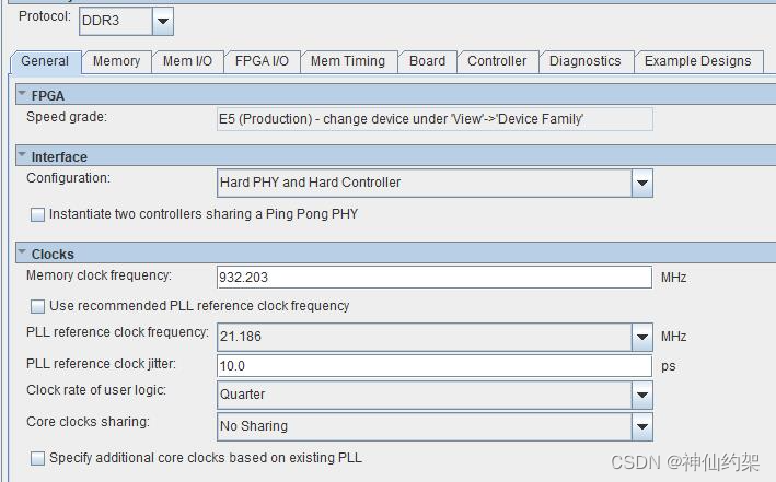
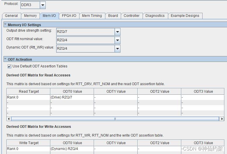
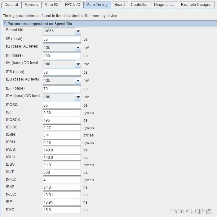
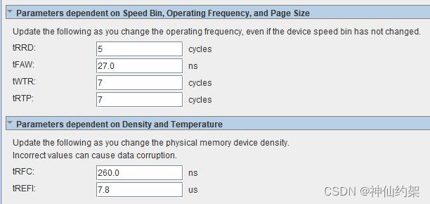
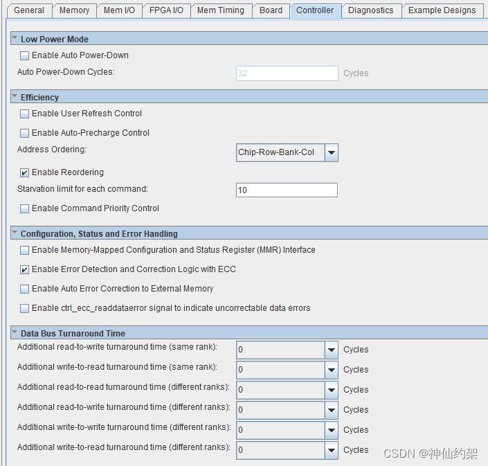
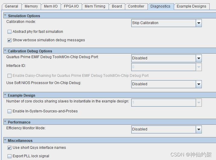
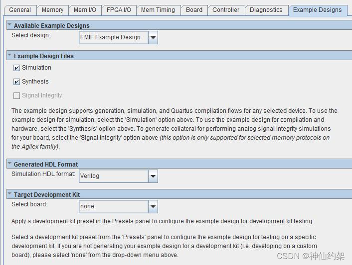
DDR IP核配置
在quartus中新建DDR测试程序,添加DDR IP,配置如下


RTL视图
调试及遇到的问题
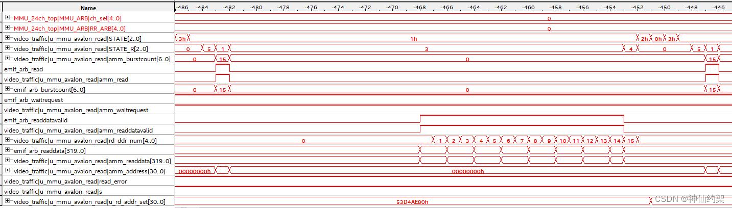
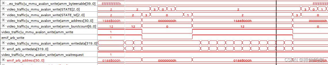
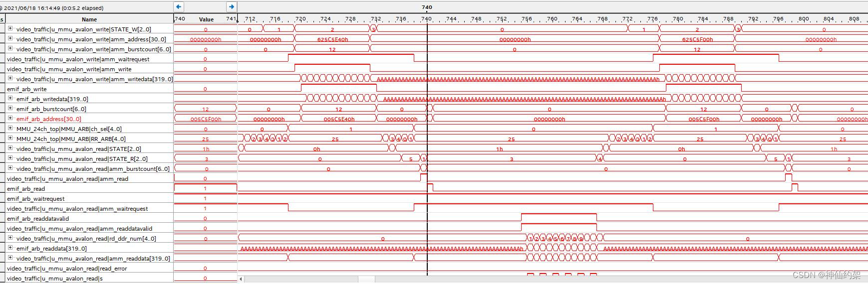
读写仲裁时序
read
burst write
多路仲裁
问题1.拉高read后,wait一直没反应

一直调不通的原因
1.文档给的时序wait的电平(高为总线繁忙)和实际是反的(高为可以传输),
2.在读写前要先判断下wait的电平,高有效的时候再发起读写
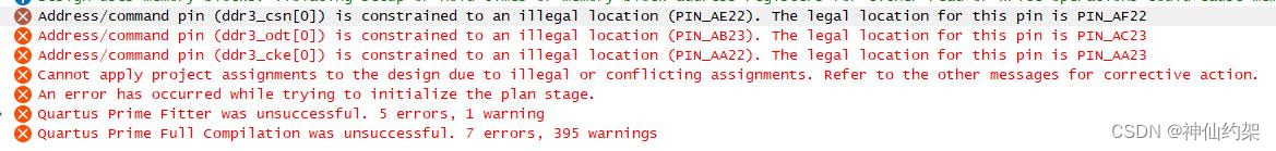
问题2.DDR校正不过的一个可能性
CSN ODT CKE接错了。
Altera DDR PHY 自动生成了管脚分配,无法更改管脚分配,去适配外部DDR的这三组接线。
延伸学习
DDR3 读写理解参考
DDR基础知识点汇总_ddr刷新周期 温度_亓磊的博客-CSDN博客
DRAM Timing · Linux Kernel Internals